Raman spectroscopy on graphene
Raman spectroscopy on graphene
Graphene, a single layer of graphite, is a material with outstanding physical properties. That two dimensional crystal was discovered by Andre Geim und Konstantin Novoselov who were awarded with the Nobel price of physics [1, 2]. Graphene can be grown on wafer-scale with high structural quality on Silicon carbide (SiC) [3]. We study both electronic and structural properties of the graphene-material system using Raman spectroscopy [4]. Raman-scattering is the excitation or annihilation of phonons by light, leading to an inelastic scattering. The photon energy shift detected by a spectrometer carries the information about the energy of the phonons created or annihilated. Figure 1 shows the spectrometer and the microscope that is used to focus the Laser light onto the sample of investigation.
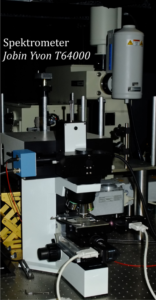
Fig. 1: Experimental setup with Raman spectrometer and microscope.
As shown in Fig 2. the scattered light is collected in the so called back scattering geometry by the use of a high aperture objective. The scattered light is directed to the spectrometer using a semi-transparent mirror (MHin Fig. 2) and focused on the entrance slit of the spectrometer. We employ a triple spectrometer, where the first two stages are used for suppression of the strong elastic back ground signal of the incoming laser radiation. After dispersion of the scattered light in the third stage, the light is spectrally resolved with a CCD-camera cooled with liquid nitrogen.
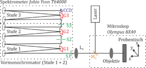
Fig. 2: Schematic experimental setup: MH: semi transparent mirror, LE: Lens used to focus the scattered light into the spectrometer, S: Entrance slit, G: Optical grating.
Fig. 3 shows a typical Raman-Spectrum of Graphene (blue Line in Fig. 3). There are two prominent Raman-lines (G-line: LO-Phonon at the center of the Brillouin-zone (BZ), 2D-line : TO-Phonon close to the BZ-border). The frequency and width of these characteristic lines yield valuable information of graphene (e.g. structural quality, carrier concentration, mechanical strain, etc.) [4, 5].
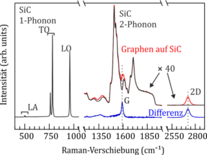
Fig. 3: Raman-Spectrum of Graphene on SiC (red). The diffference-spectrum (blue) obtained after subtraction of the SiC-Raman spectrum (black) is the contribution of the graphene layer.
Optimization of Raman-intensity of graphene on SiC
As can be seen in Fig. 4, the intensity could be enhanced by a factor of up to 20, when focusing the laser light on the back side of the SiC-substrate, rather than to the surface (conventional measurement geometry). This new geometry opens up a new field of application to study Graphene with Raman spectroscopy [6, 7].
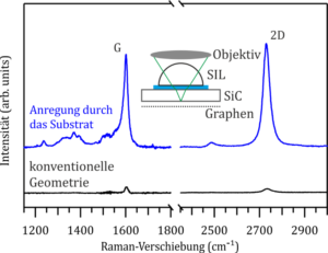
Fig. 4: Demonstration of a 20-fold intensity enhancement of the graphene Raman-signal compared to the conventional measurement geometry.
Characterization of a field effect structure of graphene on SiC
Graphene has extremely high carrier mobilities. Hence, it might be a good base material for high frequency transistors. Raman-measurements taken through the SiC substrate allow the characterization of strain and carrier mobility. The parameters of the G- and the 2D-lines as a function of gate voltage allows to disentangle the influence of mechanical strain and carrier concentration. Fig. 5 shows a typical set of Raman spectra as a function of gate voltage. [6].
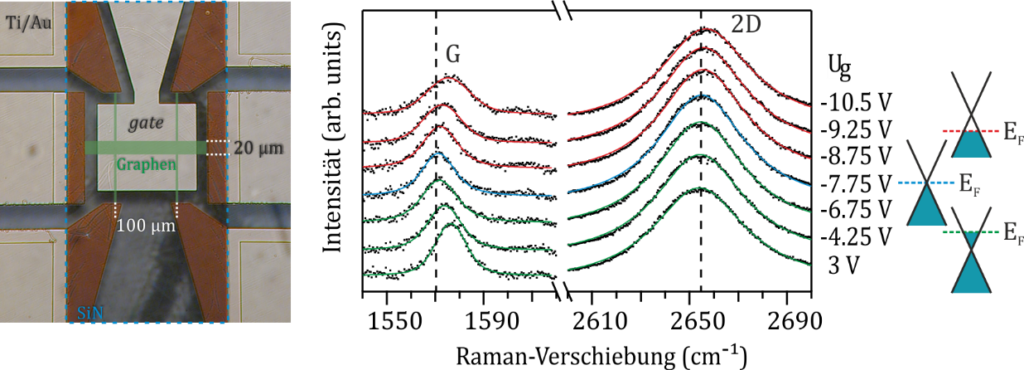
Fig. 5: left: microsopic image of a Graphene field effect transistor using Silicon Nitride as the gate dielectric and Ti/Au-Electrodes. Right: Raman-Spectra for different values of gate voltage used to control the doping of graphene.
Referenzen
[1] Novoselov et al. Electric field effect in atomically thin carbon films, Science 306, 666 (2004).
[2] Novoselov et al. Two-dimensional gas of massless Dirac fermions in graphene, Nature 438, 197 (2005).
[3] Emtsev et al. Towards wafer-size graphene layers by atmospheric pressure graphitization of silicon carbide, Nature Materials 8, 203 (2009).
[4] Ferrari und Basko Raman spectroscopy as a versatile tool for studying the properties of graphene, Nature Nanotechnology 8, 235 (2013).
[5] Fromm et al. Contribution of the buffer layer to the Raman spectrum of epitaxial graphene on SiC(0001), New Journal of Physics 15, 043031 (2013).
[6] Fromm et al. Looking behind the scenes: Raman spectroscopy of top-gated epitaxial graphene through the substrate, New Journal of Physics 15, 113006 (2013).
[7] Fromm et al. Backside monitoring of graphene on silicon carbide by Raman spectroscopy, Materials Science Forum 778-780, 1166 (2014).
